


Lithography with SPM
Пример применений 073 (pdf 600 Kb)
AFM FORCE LITHOGRAPHY
With standard silicon or silicon nitride cantilevers Force Lithography is applicable for relatively soft substrates and no qualitative change of modified surface happens but only local change of surface morphology. Electrophysical properties are not changing with this method. Fig. 1 shows the surface of polycarbonate film on a silicon substrate after force lithography. A regular array of pits has been created by rigid (Fc=40 N/m) silicon cantilever operating in the semicontact mode of AFM after the Force Lithography has been applied to points pre-set by program by bigger force under normal conditions. Distance between pits is about 25 nm. This example demonstrates the possibilities of AFM to controllable modification of the surface on nanometer scale.
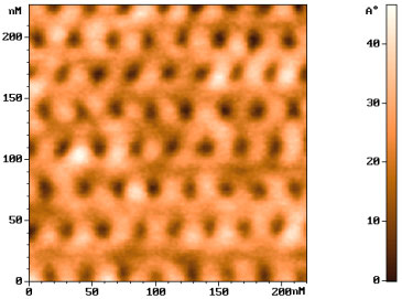
Fig. 1 AFM image of polycarbonate film surface after application of Force Nanolithography
In some cases after force lithography the convexities are observed instead of the pits. It means that a tip extracts material of the soft sample. Fig. 2 demonstrates this possibility. Drawing of the more complicated pictures is also possible. Fig. 3 shows the face, which was obtained by using raster image. Voltage lithography provides more quality image for such complex object.
For the Force Lithography on polycarbonate film semi-contact one-beam silicon cantilevers with the force constants that range from 10 to 100 N/m are recommended. Force Lithography can be execute on the surface of hard materials when special hard cantilever is used (for example, cantilever with diamond tip).
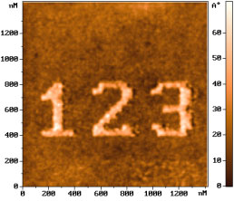
Fig. 2
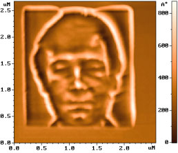
Fig. 3
AFM CURRENT LITHOGRAPHY
With the help of the Voltage Lithography not only geometrical properties of the surface can be changed but also its electrophysical properties, for example, by application of voltage to conductive cantilever the electrochemical processes on the surface can be stimulated under the Probe and, thus, material will be transformed from conductor into dielectric. On Fig. 4 abilities of tip-induced oxidation of the surface of hyperfine titanium film on silicon under normal conditions are demonstrated. It should be noted that the indicated surface area is 200 nm2, diameter of nanoparticles is 8-10 nm by the semi-height of island. It corresponds to information recording density of 0,6 Tbit/inch2.
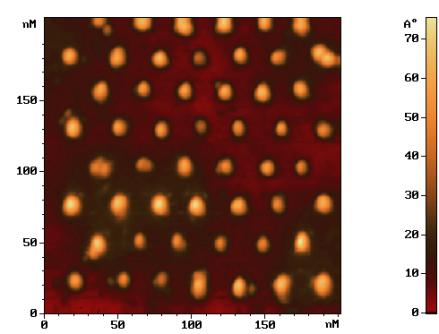
Fig. 4
Nanomodification of the surface is not limited only by formation of points. Using software we can make the Probe traveling along preset vectors and, therefore, to form lines and complex objects. Fig. 5 gives example of the Vector Lithography on titanium film through its local oxidation, which is induced by conductive tip.
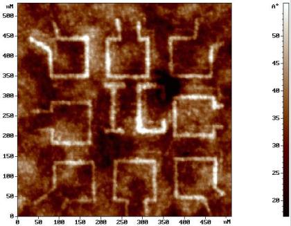
Fig. 5
The width of oxide stripe of 8-10 nanometers enables formation of tunnel-transparent barriers for electrons as well as one-electron instruments, which will operate by quantum laws even at normal indoor temperature. Lots of papers devoted to produce MIM diodes and one-electron transistors have been published [1-3]. The process of local oxidation is based on anodization. For complex pictures Raster Lithography can be execute by using file. Difference between minimum and maximum tone voltage will be applied proportionally to brightness and, correspondingly, anode oxide will grow to a different height forming different contrast of topographical image. Examples of the Raster Voltage Lithography are shown on Fig. 6 and Fig. 7. Two Nobel Laureates A. Szent-Gyorgyi (Fig. 6) and Zh.Alferov (Fig. 7) are imaged on these figures.
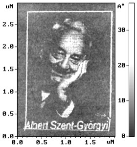
Fig. 6
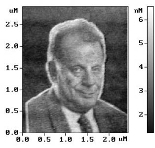
Fig. 7
SELECTION OF CANTILEVERS
To perform the Voltage Lithography on titanium film semi-contact one-beam silicon cantilever with conductive coating of high-melting alloys based on titanium and tungsten (W2C, TiO, TiN) are recommended. Type of coating does not change significantly the Voltage Lithography mode.
SELECTION AND PREPARATION OF A SAMPLE FOR THE ELECTRIC LITHOGRAPHY
To test microscope and to control program in the Probe Lithography mode we recommend to use thin titanium films on thermally oxidized silicon substrate with thickness from 1 to 10 nm. Selection of titanium as test sample is specified by electrochemical potential of anodization of up to 98% as well as its use for the Voltage Lithography described in many scientific articles [4-8]. Of course, any material, which can be electrochemically oxidized in water can be suitable for this process.We also have performed experiments to study the process of tip-induced oxidation on semi-conductors surfaces - for example on doped silicon, gallium arsenide, heterostructures and W, Nb,Al metals. Important factor in forming of the nanopattern is initial roughness of the film, which was, in our case, 0.5-2 Е. Since the height of oxide lines is only 1-6 nm, therefore, for good contrast image the film should have small irregularities. To get continuous thin and smooth films of metals and semi-conductive materials we have used methods of molecular-beam epitaxy and impulse plasma deposition.
AFM CHARGE (ELECTROSTATIC) LITHOGRAPHY
The electrization of some of samples is possible with use of disconnected cantilever. Example of the charge writing on the surface of standard silicon grating by silicon cantilever is discussed below. Fig. 8 demonstrates the topography of grating that obtained in semicontact mode after moving of the nonvibrating tip along black arrows. Existence of the charge, which was induced by cantilever friction, can explain the holes on silicon oxide (dark tracks on convexities of the grating). These holes appeared on topography owing to strong electrostatic tip-sample interaction, which displace the cantilever resonant peak during scanning in semicontact mode. This displacement leads to the cantilever amplitude changes and corresponding changes of the Z-coordinate of scanner, which is interpreted as topography. If electrostatic tip-sample interaction is attractive (the signs of probe and sample charges are contrary) then charged areas looks like holes. Repulsive interaction gives convexities on topography for charged areas. It is seen from Fig. 8 that the bulk silicon oxide (convexities of the grating) is charged contrary to cantilever.
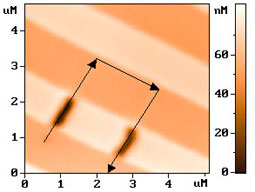
Fig. 8
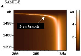
Fig. 9
Fig. 9 shows changes of the resonant peak of the cantilever during approach to the sample. On this image horizontal axis corresponds to frequency, vertical axis is Z-coordinate of scanner. Brightness corresponds to the cantilever amplitude in arbitrary units. It is seen from Fig. 9 that new branch appears when tip-sample distance becomes small. This new branch has strong dependence on tip-sample distance. The appearance of this branch can be connected with electrization, i.e. electrization is also available when oscillating cantilever strong interacts with the sample. The hole on topography after such procedure is shown on Fig. 10. The size of this hole determines minimum possible charged area for a considered sample: 200-300 nm. It is evident that minimum possible size of the charged area strong depends on material. Fig. 11 shows the example of the more complex pattern: charge signature on originally uncharged flat silicon oxide. Charge Lithography was executed in resonant mode with small tip-sample distance. It should be noted that all these charge patterns only in semicontact mode are seen. The using of the contact mode makes these charged areas invisible. Moreover, all scan will be charged after contact mode. The charged areas can be easily visualized also with Electrostatic Force Microscopy (EFM).
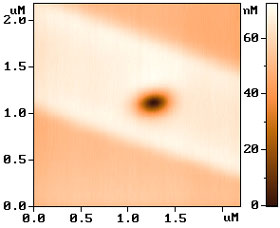
Fig. 10
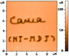
Fig. 11
REFERENCES
- J. Shiracashi, K. Matsumoto, N. Miura and M. Konagai, Single-electron transistor with Nb/Nb oxide system fabricated by atomic force microscope nano-oxidation process, Jpn.J.Appl.Phys., 1997, 36, L1257-L1260.
- K. Matsumoto, S. Takahashi et al., Application of STM nanometer -size oxidation process to planar type MIM diode, Jpn.J.Appl.Phys., 1995, 34, 1387-1390.
- K.Matsumoto, M. Ishii et al., Room temperature operation of single electron transistor made by the scanning tunneling microscope nanooxidation process for the TiOx/TiO system,Appl. Phys. Lett., 1996, 68(1), 34-36.
- Dagata J.A., Schneir J., Harray H.H., Evans C.J., Postek M.T. and Bennett J., Modification of hydrogen- passivated silicon by a scanning tunneling microscope in air, Appl.Phys.Lett., 1990, 56(20), 2001-2003.
- Nagahara L.A., Thundat T. and Lindsay S.M., Nanolitography on semiconductor surfaces under an etching solutions, Appl.Phys.Lett, 1990, 57(3), 270-272.
- Thundat T., Nagahara L.A., Oden P.I., Lindsay S.M., George M.A. and Glaunsinger W.S.,Modification of tantalium surfaces by scanning tunneling microscopy in an electrochemical cell, J.Vac.Sci.Technol., 1990,A 8(4), 3537-3541.
- Garcia R., Calleja M. and Perez-Murano F.,Appl.Phys.Lett1998, 72, 2295.
- Ph. Avouris, T.Hertel, R. Martel, Atomic force microscope tip-induced local oxidation of silicon: Kinetics, mechanism, and nanofabrication. Appl. Phys. Lett., 1997, 71(2), 285-287.