


Optical Imaging and Spectroscopy at the Nanometer Scale
Application Note 099 (pdf 580 Kb)
SNOM applications in the following areas are presented:
- Laser emission
- Optical fibers
- Optical micro-devices Plasmonics
- Photonic crystals and waveguides
- Photovoltaics
- Polymers
- Quantum Dots
- Scattering (Apertureless-) SNOM
Scanning near-field optical microscopy (SNOM) enables studying a sample’s optical properties with resolution far beyond the diffraction limit. Sample fluorescence, light emission, transmission, scattering etc. can be mapped with the spatial resolution down to tens of nanometers.
Two main approaches to the near-field microscopy exist: aperture type SNOM and apertureless techniques.
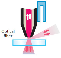
SNOM based on quartz fibers
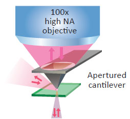
SNOM based on silicon cantilevers with nanofabricated aperture
In the first case, a subwavelength size aperture on a scanning tip is used as an optical probe. This is usually an opening in a metal coating of either an optical fiber tip or of a cantilever. Spatial resolution in the aperture type SNOM is, in general, determined by the aperture diameter.
Apertureless techniques are based on the near-field optical phenomena as well, but do not require passing the light through an aperture. Apertureless/Scattering SNOM, Tip Enhanced Raman/Fluorescence, STM Light Emission and others fall into this category.
SNOM techniques are widely used in nanophotonics (plasmonics, photonic crystals & waveguides etc.), laser technology, optical micro-devices and material science.
NT-MDT SI SNOM FEATURES
All major types of SNOM probes and measuring modes supported.
Apertured cantilevers, different types and shapes of apertured optical fibers and even sharpened metal wires can be used as SNOM probes. Major SNOM measuring modes are: Transmission, Collection and Reflection. Signals measured: laser intensity, fluorescence intensity and full emission spectra.
Apertureless techniques: Scattering SNOM, Tip Enhanced Raman/Fluorescence and others.
In general, all types of optical, mechanical, and electrical interactions between the probe, sample and incident light source can be studied by NT-MDT SI SNOM setup.
HybriD optical measuring mode:
In this mode tip-sample distance is periodically modulated. Tip gets in and out contact with the sample thousand times per second. Optical signal resulting from the tip-sample interaction is continuously measured and recorded for each approach-retract cycle by fast electronics. The resulting multi-dimensional data (optical signal vs. tip-sample distance in each XY scanning point) presents, upon proper postprocessing, unique information about near-field and far-field components of the optical signal. This allows
increasing SNOM measurement sensitivity and resolution.
Scanning by sample and/or by probe.
Depending on the type of sample and measurement, it is important to have the option to scan either by the sample or by the probe to obtain SNOM images.
Environmental control (temperature, gases, humidity, liquid and external magnetic field).
Temperature control and air flow isolation are the key issues for measurements stability. Sample heating and controlled gas atmosphere removes the residual water layer on the sample (this is usually present in ambient conditions and affects any surface measurements). This prevents unwanted chemical reactions on the surface and other measurement artifacts.
Extended spectral region (UV – Vis – IR).
Standard supported wavelength range is 400-1700 nm. Customized solutions for wider ranges are possible.
Easy integration with AFM & confocal Raman microscopy.
Universal NT-MDT SI NTEGRA SPM base allows one to switch easily between any types of AFM/STM/SNOM measuring heads and environmental cells. The setup can be further integrated with a Raman spectrometer to provide simultaneous AFM/Confocal Raman & fluorescence imaging in addition to SNOM.
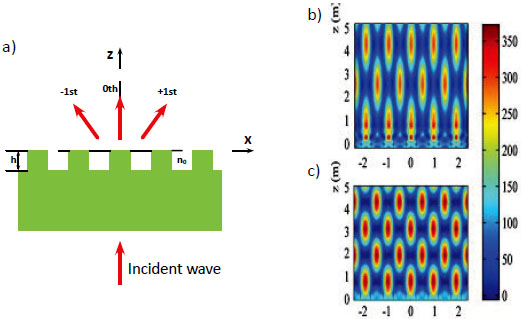
SNOM IMAGING FOR LASER STUDIES
Study of Laser Emission Properties SNOM can be effectively used to study laser emission properties.
Both near-field (right at the laser facet) and far-field (at a certain distance from the facet) emission patterns can be obtained with high spatial resolution (<50 nm). Both emission intensity and full emission spectrum can be recorded during a 2D or 3D optical scan.
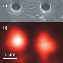
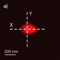
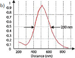
Fig. 1. (a) Side view SEM image of a verysmall-aperture-laser (VSAL) facet with an annular aperture (left) and a circular aperture (right). (b) Intensity distribution of the light emission (at 650 nm) detected at the surface of the VSAL facet. Data from: Hongfeng Gai, Jia Wang, APPLIED OPTICS, Vol. 46, No. 25, 1 September 2007
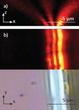
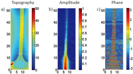
Fig. 2. (a) XZ section of the intensity distribution of the light emission (at ~1070 nm wavelength) from 0 to 4.5 μm above the surface of a cleaved laser. (b) Near-field intensity distribution of the light emission detected at the surface (top half) and optical image of cleaved laser (bottom half). Data from: A. Shelaev, M. Yanul, NT‑MDT SI. Sample courtesy: A. Ankudinov, S. Slipchenko, A. Podoskin, I. Tarasov, Ioffe Physical Technical Institute
SNOM FOR OPTICAL FIBERS
Broadband Emissions from γ-AL2O3 Nanocrystals in Cr-Doped Double-Clad Fibers
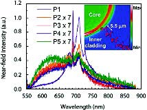
Fig. 3. Near-field spectra and corresponding SNOM mapping of the inner cladding and core of the Cr-doped double-clad fiber. The spectra show the broadband properties, their bandwidth and intensity, which are of concern for a potential optical coherence tomography light source. These spectra present the dependence on the radial distributions of Cr3+:γ-Al2O3 nanocrystals and clusters. Data from: Chien-Chih Lai, Shih-Chang Wang, Yen-Sheng Lin, Ting-Hao Chen, and Sheng-Lung Huang, JOURNAL OF PHYSICAL CHEMISTRY C, 115, 20289–20294 (2011)
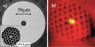
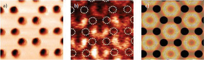
Fig. 4. (a) SEM image of the optical fiber cross-section, showing photonic crystal structure in the fiber core. (b) Overlay of topography map (red palette) and light intensity (SNOM collection) image (green palette) taken from the fiber section. Light propagating in the fiber is perfectly localized in the center of the photonic crystal structure. Data from: Yinlan Ruan, Heike Ebendorff-Heidepriem, Tanya M. Monro, Centre of Expertise in Photonics, School of Chemistry & Physics, University of Adelaide
SNOM FOR OPTICAL MICRO-DEVICES
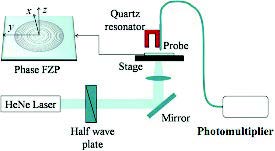
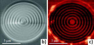
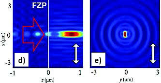
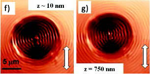
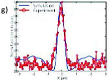
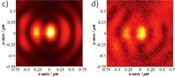
Near-field Focusing of a Phase Micro-Fresnel Zone Plate.
Focusing behavior of a binary phase micro-Fresnel zone plate (FZP) fabricated using focused ion beam milling on a glass substrate is studied by SNOM. It is found that an asymmetric spot with subwavelength beam width and elongated depth of focus can be obtained from the phase micro-FZP. The measurements are consistent with calculation results.
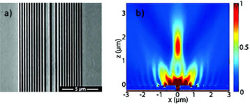
Characterization of a Micro-focusing Plasmonic Device.
Focusing behavior of Au based focusing plasmonic device is characterized by SNOM. The experimental results show a significant focusing effect in agreement with the simulation results.
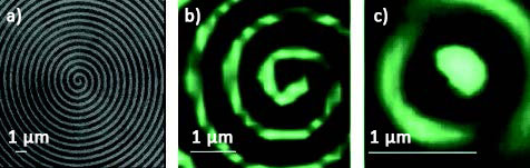
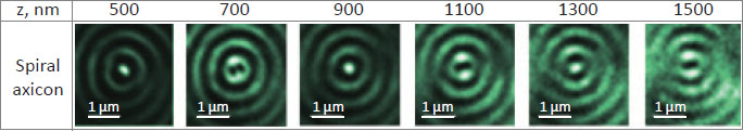
Light Spot Narrowing by an Assymetric Axicon.
Diffraction of a Gaussian beam by axicons is studied by SNOM. Binary diffraction axicons with the period close to the light wavelength are formed by electron beam lithography on a quartz substrate. Different axicon geometries are studied. It is shown experimentally that asymmetric microaxicon can reduce the spot size of central light beam along polarization direction in a near zone of diffraction – overcoming the diffraction limit.
Focusing of a Radially Polarized Beam by a Solid Immersion Lens.
Radially polarized beam focused by a solid immersion lens (SIL) is studied by SNOM. It delivers a laser spot beyond the diffraction limit demonstrating better focusing properties than a common linearly polarized beam.
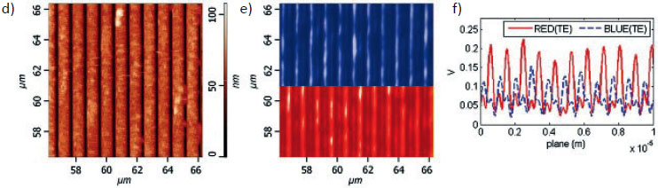
Color Separation in the Fresnel Diffraction Region of Rectangular Grating.
Color separation of the incident light in the Fresnel diffraction region is a novel function of high-density dielectric rectangular gratings. Light of different wavelengths has different diffraction periods in the Z direction. For example, at 4.2 μm distance from the surface, position of intensity maximum for red excitation laser corresponds to position of intensity minimum for blue excitation laser - a spatial light separation occurs.
SNOM FOR PLASMONICS
SNOM is traditionally used to examine the Surface Plasmon Polaritons (SPP) behavior with high spatial resolution in all three dimensions (XYZ).
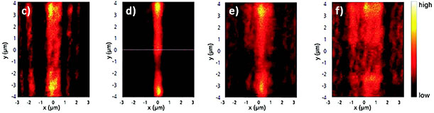
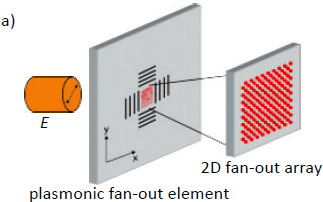
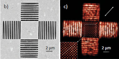
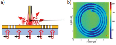
Plasmonic Fan-Out.
SPP behavior is often studied in relation to conventional optical devices such as beam splitters and waveguides. The work conducted by Wang et al. (Fig. 10) realizes traditional fan-out optical arrangement in a plasmonic device. An optical fan-out element typically splits a single wave into plane waves by using gratings and lenses to generate an array of light spots.
A plasmonic fan-out array is generated by the structure shown in Fig. 10 (a, b). The device is produced using arrays of slits on a metal film, the slits being of less than the wavelength dimensions of the initial light. The structure consists of a 100 nm silver film deposited on a quartz substrate. The slit arrays are cut into the silver film by electron beam lithography (EBL) at a width of 265 nm to generate the highest surface plasmon response. The near field characteristics of the SPP pattern are investigated
by SNOM with an aluminium coated fiber tip. The results of the imaging analysis are shown in Fig. 10 (c).
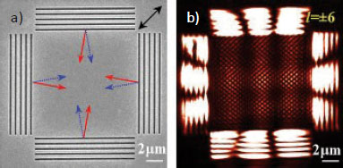
Generation of Plasmonic Moiré Fringes Using Phase-engineered Optical Vortex Beam.
The work demonstrates the dynamic generation of two dimensional (2D) plasmonic Moiré fringes resulting from the overlapping of two Surface Plasmon Polaritons (SPP) standing waves with an angular misalignment. The SPP waves are excited by an optical vortex (OV) beam with different topological charges (l= ±6). The sign of l determines handedness of the helical wave front. Due to their unique phase properties, OV beams provide a natural and simple phase modulation method to effectively and dynamically
manipulate SPPs.
Guided Plasmons on a Gold Waveguide.
Surface plasmon polariton (SPP) propagation in an SPP waveguide is studied using SNOM equipped with a heterodyne interferometer. Both intensity and phase distribution of SPP electromagnetic field are measured.
SERS Substrate.
Polarization-Controlled Tunable Directional Coupling of Surface Plasmon Polaritons.
The polarization states of the optical signal that can be coupled to a plasmonic device are often limited by the selectivity of the coupling process. For directional SPP excitation, usually only the component of the incident light that is polarized perpendicularly to either groove- or ridge-like scattering elements (in the case of gratings) or to the metal surface itself (in the case of prism-based schemes) can be coupled into SPPs . Light in the orthogonal polarization does not couple to SPPs, leading to a decrease
in the SPP signal and a loss of information about the incident polarization state.
Additional challenges arise in controlling the direction of propagation of the generated SPPs. Usually the direction of propagation of generated SPPs is difficult to control, that results in a substantial source of noise and reduces efficiency. This work presents a directional plasmonic coupler that addresses these challenges by offering polarization-invariant coupling efficiency to SPPs while allowing full control over the distribution of power between two counterpropagating SPP modes. This includes unidirectional coupling and preserves polarization information. A special structure was fabricated in a 150-nm-thick gold film using focused ion beam milling (FIB). The structure was backilluminated with polarized 633-nm laser light, and the SPPs were measured using scanning near-field optical microscopy.
SNOM FOR PHOTONIC CRYSTALS
Light Propagation in a Photonic Crystal Waveguide.
Aperture-SNOM in collection mode is used to correlate the electromagnetic field distribution with the surface topography of the photonic crystal. The optical near-field confined above the sample surface is collected by a SNOM tip, placed several nanometers above the sample surface.
Data from: R. Geiss, S. Diziain, N. Janunts, APPLIED PHYSICS LETTERS 97, 131109 (2010)
Analysis of Slow Bloch Modes in a Photonic Crystal
The photonic crystal is prepared by drilling a honeycomb lattice of air holes in the InP slab using e-beam lithography followed by reactive ion etching. Near-field optical microscopy is used to visualize the evanescent component of the mode with a spatial resolution below the diffraction limit.
SNOM FOR PHOTOVOLTAICS
Localized SNOM Excitation for Solar Cell Studies.
SNOM is used for localized optical excitation of a monocrystalline silicon solar cell. Topography, local surface reflection and localized photoresponse of the cell are simultaneously mapped while scanning with the SNOM probe. This allows characterizing near-surface defects and other optoelectrical properties of the cell with high spatial resolution and correlating them with the surface topography.
SNOM FOR POLYMERS
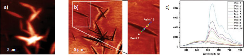
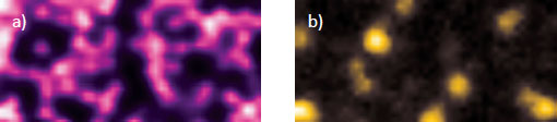
Perylene Embedded in Polyfluorene.
Perylene (a small-molecular organic semiconductor) was embedded in Polyfluorene (PFO) polymer organic semiconductor thin film forming a rhombus structure. SNOM transmission spectroscopy scheme was used to study the optical proprieties of the structure. It is known that fluorescence properties of perylene nanosheets directly relate to their crystal structures. For β-phase rhombus perylene, the fluorescence peak is around 620 nm, which can be clearly observed from fluorescent spectra along the section on the SNOM
image. Excitation laser wavelength was 473 nm.
SNOM FOR QUANTUM DOTS
For high resolution photoluminescence (PL) studies of quantum dots (QDs) grown on non-transparent substrate the so-called illumination-collection SNOM regime is most efficient. In this regime, both laser illumination and PL signal collection are performed through the same SNOM probe nano-aperture. Proper design of the probes (high transmission), optimized experimental setup (good collection optics) as well as right measuring procedure (ensuring that probe is in near-field optical regime with the sample) allow efficient optical excitation and detection of individual QD PL.
SCATTERING (APERTURELESS-) SNOM
Scattering (apertureless) SNOM technique is usually used to visualize localized electromagnetic field in plasmonic structures. In this technique, a sharp probe is used to scatter localized near-field light into the far field. The scattered radiation intensity is measured in far field while tip scans over the sample surface, thus visualizing distribution of light localized in the structure with spatial resolution ~10 nm.
NT-MDT SI SNOM SPECIFICATION
SNOM & other probes
SNOM optical fibers; SNOM apertured cantilevers; All types of AFM cantilevers; Sharp metal wires
Supported standard modes
SNOM modes: Transmission; Collection; Reflection; HybriD mode (optical signal vs. tip-sample distance recording) for multi-dimentional optical imaging
AFM modes*: >30 modes (MFM, SKM, SCM, SRI, LFM, EFM, SThM, UFM, PFM, AFAM and others)
Detected optical signals
Laser intensity; Fluorescence intensity; Spectroscopy (full spectrum at each point)
Excitation/detection wavelength range
400 – 1700 nm; Customized solutions for wider ranges are possible
Advanced near-field modes and techniques
Scattering SNOM (s-SNOM); Apertureless SNOM (a-SNOM); Tip Enhanced Raman Scattering (TERS); Tip Enhanced Fluorescence Spectroscopy (TEFS); SNOM lithography (vector, raster); Light emission/absorption at AFM/STM gap; Polarization microscopy
Optical detectors
Photon multipliers (VIS, IR); Spectrometer with TE cooled CCD camera; Avalanche photodiodes (photon counting regime)
Scanning and feedback mechanisms
Scan by tip & scan by sample regime (100 x 100 μm) High resonance XYZ piezotube for fast scanning (closed-loop feedback); Flat piezo-driven scanning stage (closed-loop feedback)
Laser based cantilever deflection detection (VIS or IR laser); Quartz tuning fork resonator force detection system (shear force & normal force regimes)
Other features
Easy upgrade/integration with confocal Raman/Fluorescence microscopy
Automated alignment of laser spot to aperture of SNOM cantilever
Very high efficiency (numerical aperture) excitation/collection optics
Environmental control: temperature, humidity, gases, liquid, magnetic field
Compatible with commercially available inverted optical microscopes
*May require different types of probes. When probes are exchanged, exact area of the sample is kept within μm precision