


Characterization of Materials with a Combined AFM/Raman Microscope
Application Note 089 (pdf 3.3 Mb)
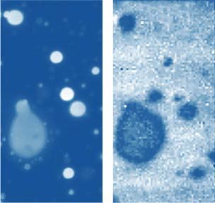
Topography and Raman Map of PS in PS/PMMA blend
- Introducing a combined AFM/Raman instrument based on Raman Confocal microscope DXR (Thermo Fisher Scientific) and NTEGRA Spectra Unit (NT‑MDT SI).
- Basic questions regarding the sensitivity, lateral and axial resolution and Tip-Enhanced Raman Spectroscopy measurements are discussed in this publication.
- The capabilities of Raman Spectroscopy and Atomic Force Microscopy were verified on multilayered samples. polymer blends, wooden cells and ultrathin polymer films
Marko Surtchev1, Sergei Magonov1 and Mark Wall2
1NT-MDT America, Tempe, AZ U.S.A.
2Thermo Fisher Scientific, Madison, WI, U.S.A.
INTRODUCTION
Comprehensive material characterization requires the examination of samples by multiple complementary techniques. This task becomes more challenging for analysis of heterogeneous materials at small scales. Understanding the relationship between sample morphology and their technological properties is the cornerstone in the development of novel materials. The strong interest in chemical identification of components at the microscopic scale has motivated the development of infrared and Raman microscopes. The identification of individual constituents in multicomponent polymer systems and mapping their distribution becomes a challenging task when the dimensions approach the sub-micron and sub-100 nm scales. Atomic force microscopy (AFM) is the most developed scanning probe technique and it provides the researcher not only with topographical information down to the atomic scale but also enables the quantitative measurements of local mechanical and electromagnetic properties. In regards to the compositional imaging of heterogeneous materials, AFMbased studies rely on the specific shape and dimensions of individual constituents and differences in their local mechanical, electric and thermal properties. The compositional AFM maps of block copolymers, polymer blends, incomplete metal alloys and semiconductor structures are well documented [1-2]. However, the identification of the individual components based purely on AFM studies in these complex materials is primarily indirect and has definite limitations. Integrated instrumentation coupling spectroscopic techniques such as infrared and Raman with AFM provides a means to obtain direct and specific insight into the chemical nature of the
constituents of complex materials.
In a combined measurement with an AFM microscope and a Raman spectrometer surface profiling and measurements of local materials properties can be performed simultaneously with the collection of Raman maps component-specific molecular information. We will describe the AFM/Raman confocal microscopy studies of a number of heterogeneous materials combined with mapping of their mechanical and electric properties. Currently, combined AFM/Raman in struments are more common and commercially available compared to emerging AFM/IR devices. The coupling of the two microscopic techniques provides two main benefits. The first benefit is simultaneous AFM and spectroscopic measurements in the same sample area.
The second benefit that the combined technique provides is the capability of advancing the spectroscopic mapping to sub-100 nm scale using the local enhancement of the electric field in socalled tip-enhanced Raman scattering (TERS) measurements [3]. In the AFM/Raman work presented below we will focus on the first aspect, the information and benefits obtained by performing simultaneous and co-incident AFM/Raman measurements. Several important details of these measurements such as lateral and depth resolution
will be discussed in studies of binary polymer blends. The complementary nature of the AFM and Raman measurements will be illustrated with the experiments on composite materials and semiconductor structures.
INSTRUMENTATION AND IMAGING ROUTINES
The integration of the Thermo Scientific DXR confocal Raman microscope (Thermo Fisher Scientific) with
the Scanning Probe Optical Unit (NT‑MDT SI) is shown in Figure 1. The DXR Raman microscope can be configured with 3 different lasers (Green (532 nm), Blue (455nm) and Red (633 nm)) and can be used in a combined AFM/Raman operation, or each instrument can be operated independently. Through space optics are employed to direct a well collimated laser beam from the DXR microscope to the entrance of the scanning probe unit. In the SPM unit, the beam is reflected by a system of mirrors, one of which is installed on a closed-loop piezo-scanner. Finally, the beam is brought down to the scanning probe head where it hits the sample. The beam position is controlled by a piezo-drive mirror is focused with a N/A = 0.75 lens. The piezo controlled mirror is used for fine positioning of the laser beam on the sample’s region of interest or at the tip apex. The Raman light scattered from the sample positioned on the scanning probe unit is collected at 180 degrees and sent through the same through space optics back to the entrance of the Raman microscope’s spectrograph. Another scanner pivots the sample under the AFM probe. The scanning probe unit enables the scanning tunneling microscopy or atomic force microscopy (AFM) measurements.
In an AFM operation, the unit incorporates a laser detection system that is used for monitoring the probe-sample interactions by measuring a reflected beam bounced from the probe cantilever. The laser and the light deflected from the cantilever use the same optical path as the Raman probing laser. In the experiment an operator directs the AFM laser onto the cantilever and positions the resultant reflected beam from the cantilever onto a photodetector. After this alignment is accomplished the sample is brought into close proximity with the probe where an interaction between the probe and sample takes place and collection of AFM data is poised to proceed.
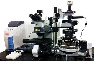
Fig. 1. DXR Raman microscope (Thermo Fisher Scientific) with NTEGRA Spectra unit (NT‑MDT SI)
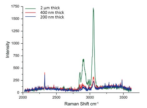
Fig. 2 Raman spectra of films of different thickness prepared of a blend of polystyrene and linear low density polyethylene. Acquisition time - 60 sec. He-Ne laser (633 nm emission) was used
Next the Raman laser is positioned in the vicinity of the AFM tip at which point the collection of AFM and Raman data can begin. In the scanning process, the scanner moves a sample under the probe, the AFM and Raman data are collected simultaneously from the same sample area. The use of an AFM microscope provides the researcher with the most complete set of the techniques including non-resonant oscillatory Hybrid (HD) mode [4], single- and double-pass electric measurements in Amplitude Modulation mode (AM), high-voltage piezoresponse microscopy in contact mode and others. In the studies described in this note topographic imaging was performed mostly in AM mode, and the local mechanical and electric studies were made in HD mode and single-pass Kelvin force microscopy modes. In HD mode a sample is brought into intermittent contact with the probe by oscillation at frequency well below the resonances of Z-scanner and the probe. The probe bending at the frequency is measured and its maximal value, which is set by an operator, is used for the feedback control during scanning the sample. The deflection cycle in this mode contains information regarding local mechanical and other properties, which are detected andvmapped simultaneously with the surface topography.
Optimization of the instrument for AFM/Raman measurements involves the collection of the spectral and topographic data from the same spot, as well as the issues related to sensitivity, spatial resolution and collection time. In addition to the positioning of the laser beam of the Raman microscope at the probe locations, it is important to use probes with a tip designed to minimize shadowing of the laser by a cantilever. AFM is superior in spatial resolution and extends the visualization of surface structures down to the molecular scale. In contrast with Raman scattering, the wavelength of laser light defines the sample volume from which light scatters. This volume has a diameter that varies from 300 nm to 1 micron depending on the wavelength of the excitation light and this is a critical factor determining the spatial resolution of conventional Raman microscopes. The collection of Raman scattering signal from polymer films that occupies only a part of the scattering volume needs longer collection times. This is illustrated in Figure 2, where one sees the spectra obtained for
polymer films of different thickness at the same acquisition time.
Most of the results presented in this Application Note were obtained on the micron scale in traditional AFM/Raman measurements. They are limited to sub-micron lateral and depth resolution. Sub-100 nm mapping can be achieved with Tip Enhanced Raman Spectroscopy (TERS). This phenomenon is related to the enhancement of local electromagnetic field in the immediate vicinity of Au- or Ag-coated tips, and it is well documented in measurements on low-dimensional carbon materials, such as graphene, carbon nanotubes, etc. In regards the TERS studies of other materials (e.g. polymers, organics, bioobjects) there are a limited number of published reports and the technique has not become routine yet. The main hurdles limiting the use of this technique are related to the tip quality, reproducibility and longevity. Currently, a large amount of effort is undertaken towards
TERS probe preparation and optimizing the imaging procedures for mapping a broader range of samples.
COMBINING AFM AND CONFOCAL RAMAN STUDIES
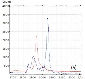
Confocal Raman measurements provide unique detailed and specific chemical information by placing an aperture at the back focal plane of the microscope objective. The aperture improves the spatial resolution of the microscope and enables depth profiling by acquiring spectra as the laser focus is moved into a transparent sample. In Raman microscopes, this motion is typically performed with a stepper motor and the axial resolution is limited to ~2 microns. The change of the Raman spectra during the depth profiling of a packaging film is shown in Figure 3a. This figure reveals the layered structure of the sample that composed of different polymers [5]. In concert with an AFM microscope these Raman studies can be enhanced by a precise vertical motion of a piezo-scanner, which is applied for the positioning of the laser focus.
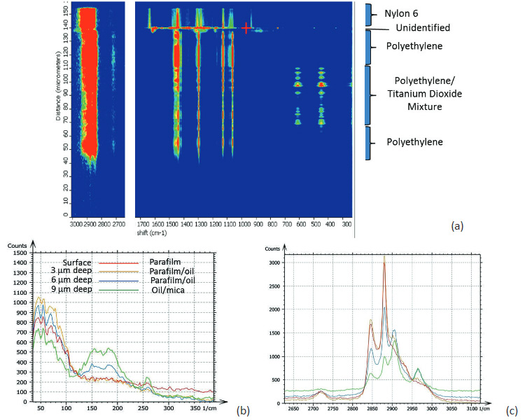
In a related application several spectra were acquired at different depths into a “sandwich” sample made by
placing silicon oil between mica and a paraffin film. The results are shown in Figures 3b-c. The spectra
were collected in two spectral regions on the surface and at depths of 3, 6 and 9 microns. A gradual change
of the spectra reflects the layered structure of the 3-component sample.
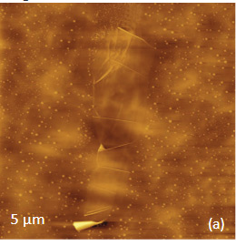
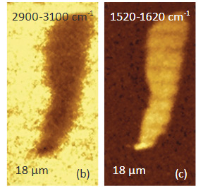
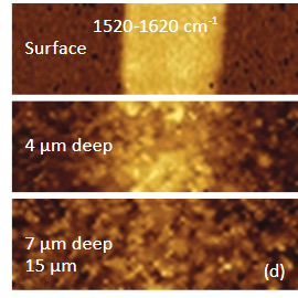
Another confocal measurement on a sample of poly (vinyledene fluoride) - PVDF film with graphite flakes is shown in Figure 4. The height image of the surface of an area with a flat lying flake in the center is shown in Figure 4a. The flake can be faintly seen in the optical image, being distinguished by some “wrinkles” and by the absence of grainy structures that cover the surrounding areas. Clear differentiation between the flake and the polymer is obtained in Raman scattering maps (Figures 4b-c) in the wavenumber
regions specific for these components (2900 cm – 3100 cm‑1 region (C-H) for PVDF and the 1520 cm‑1 – 1620 cm‑1 region (G-band) for graphite). The Raman maps of the intensity of the 1520 cm‑1 – 1620 cm‑1 band at different depths point out that thickness of the graphite
flake is around 4 micron, Figure 4d.
Polymers exhibit Raman scattering bands which are uniquely related to their chemical bonds. Therefore,
the identity of the individual components of polymer blends using Raman scattering signals at chemically-specific frequencies in combination with AFM imaging providing valuable information that establishes the chemical-morphology-property relationship in these industrially important materials.
To demonstrate the information that Raman provides a polymer blend of two immiscible components was prepared by mixing polystyrene (PS) and poly (vinyl acetate) together. The Raman spectra of these polymers in the C-H spectral region are shown in Figures 5a-b.
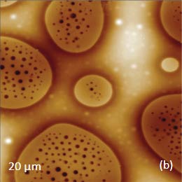
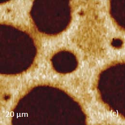
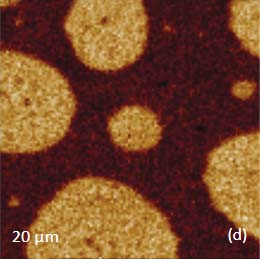
The Raman bands at the PVAC-specific region: 2839 cm‑1 – 2980 cm‑1 and PS-specific region: 3000 cm‑1 – 3140 cm‑1 clearly show distinct differences and can be used to identify the distribution of these polymers in the polymer blend. The height image of the film on the PS/PVAC blend on Si (Figure 5c) shows the perforated protrusions and matrix. This morphology hints at a microphase separation of the individual constituents. A comparison of the intensity maps for the chosen Raman scattering bands points out that the protrusions are composed of PS and the matrix PVAC (Figures 5d-e). Numerous “droplets” are seen between the protrusions in the height image but only the larger of these features are distinguished in the Raman map in Figure 5e since the smaller features are below the diffraction limit of the resolution of Raman microscopy.
Prior to the development of AFM/Raman microscopes the compositional AFM imaging of the polymer blends was performed using phase contrast [1]. With this mode of operation, the phase images differentiate the individual components of polymer blends due to the phase changes that the probe experiences during the interaction with dissimilar materials. The height and phase images of a film of an immiscible blend of PS and polybutadiene (PBD) blend are shown in Figures 6a-b.
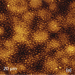
The binary contrast of the phase image suggests that the round elevated domains and surrounding matrix seen in the height image can be assigned to different components of the properties of polymer materials and phase contrast have often been employed for assignment of locations with different phase contrast. As discussed above the addition of Raman scattering to AFM provides a direct means for chemical identification of the components of the polymer blends. The Raman maps of the scattering bands in the region of C-H bonds (2814 cm‑1 – 2963 cm‑1 PBD) and (3025 cm‑1 – 2094 cm‑1 PS) indicate that the matrix is made up of PBD and the elevated protrusions are of PS (Figures 6cd). A comparison of the phase image (Figure 6b) and the map (Figure 6d) show higher spatial resolution of the phase imaging. The differences in the spatial resolution of AFM and conventional Raman mapping is also seen from a study of a film of immiscible blend of PVDF and poly(methyl methacrylate) – PMMA.
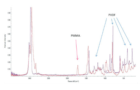
The Raman spectra of the polymers were taken from the Thermo Fisher spectral library (Figure 7a), and they have a number of bands, which can be used for differentiation of these components in binary blends made from these materials. We have chosen the 770 cm‑1 800 cm‑1 (C=O) band for PMMA identification and the 1700 cm‑1 – 1760 cm‑1 band for PVDF identification. The bands are resolved in the Raman spectrum of PMMA/PVDF blend, Figure 7b.
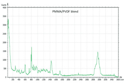
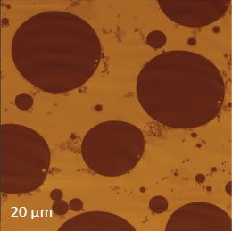
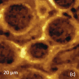
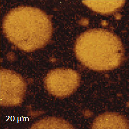
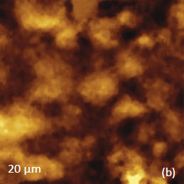
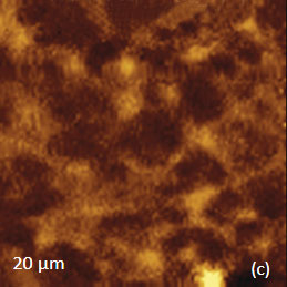
The AFM/Raman data obtained from this film are shown in Figure 8a-c. The height image shows that the film is characterized by a combination of small sub-micron particles, which densely cover the whole area, and larger round-shaped domains with dimensions in a few microns range.
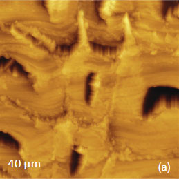
The Raman maps present variations of intensity of PMMA and PVDF bands and distinguish only the round-shaped domains and areas inbetween. These domains are identified as PVDF and the surrounding matrix is composed of PMMA. Small particles covering the surface are not invisible in the Raman scattering maps. This makes their identification quite challenging. In this case we would expect that TERS measurements will be able to provide more detail about the identity of the smaller particles by virtue of the technique’s sub-100 nm spatial resolutions. Visualization of species in composite materials is also improved by AFM/Raman mapping. Imaging plant cell provides a good example demonstrating the valuable and detailed information AFM/Raman provides. Plant cells are heterogeneous natural nanocomposites formed of cellulose, lignin and hemicelluloses. Insight into the structure of this material is important to understand the mechanical, chemical and biological features of plants and plant materials. Raman microscopy has been used for the study of the distribution of lignin and cellulose in the cell walls of woody tissue [6]. An example of a combined AFM/Raman measurement of wood cells is given in Figure 9ac.
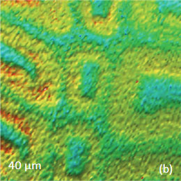
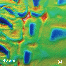
The red spots correspond to high intensity, the blue spots – to low intensity
Height image shows an array of cells with partially empty cell cores that are surrounded by multilayer walls (Figure 9a). Raman scattering maps show the distribution of Lignin and cellulose (Figures 9b-c), where the image intensities are based upon the component specific vibrational bands of lignin and cellulose (380 cm‑1 and 1600 cm‑1, respectively). In these maps the locations with high/low concentration of cellulose and lignin are show in red/blue, respectively. These components are localized mostly in the cell walls yet their lateral distributions are quite different. More detailed analysis of the lignin/cellulose ratio in different layers surrounding the cells is given in [6].
INTERPLAY BETWEEN NANOMECHANICAL AND AFM/RAMAN MEASUREMENTS
The quantitative measurements of local mechanical properties such as elastic modulus and work of adhesion in complex materials have become more of a routine procedure thanks to recent developments of HD mode.
In this mode nanomechanical data can be recorded in a single point or over an area to get the maps (up to 1024×1024 pixels) of these properties. The variation in elastic modulus of polymers span over the several decades from several kPa up to 10 GPa.
Like phase contrast maps, mapping of elastic modulus can also be used for compositional imaging of polymer blends. However, in studies of ultrathin (thickness below 100 nm) polymer films on rigid substrates the situation is more complicated. Here one should take into consideration the influence of the substrate on the mechanical properties of the films.
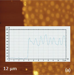
As an example consider the ultrathin film of PS/PBD film on Si substrate Figure 10. The height image reveals the common morphology of immiscible blends that is composed of number circular domains in a surrounding matrix as seen in the right side of the image in Figure 10a. The underlying Si surface, which was opened with a scratch, can be seen in the left side of the image. The height profile taken across the imaged area (center insert) shows that the circular elevated domains are 50-80 nm in height and the matrix is ~40 nm in height.
The elastic modulus map (Figure 10b) of this sample was recorded in the HD mode and reveals that the elastic modulus of the circular protrusions is lower than that of the matrix.
They both exhibit moduli, which are closer to the elastic modulus of bulk PS (2-3 GPa) than to the elastic modulus of PBD (~16 MPa). These maps were obtained through the on-line analysis of the 64’́64 arrays of force curves in the framework of Deruigin-Muller-Toporov deformation model.
The rational understanding of these results is impossible without the Raman map of the PS band (Figure 10c).
The map allows the direct assignment of the elevated domains to PS and the matrix to PBD. This information indicates that the measurements of elastic moduli of these thin films are influenced by a substrate effect and explains the slightly stronger deformation of PS domains, which are slightly higher than the PBD surrounding. The latter is substantially reinforced by the underlying Si substrate.
COMBINING LOCAL ELECTRIC MEASUREMENTS AND AFM/RAMAN STUDIES
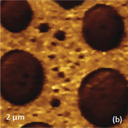
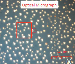
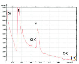
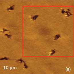
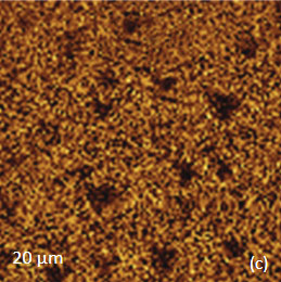
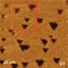
The family of AFM techniques includes methods for measurements of local electric properties such as single-pass studies of surface potential (Kelvin force microscopy – KFM). A joint experiment of KFM and AFM/Raman imaging was performed on a sample of Si (111) covered with polycrystalline Si-C film of 80 nm in thickness. The optical view of the Si-C/Si in Figure 11a exhibits multiple triangular pits, which can be assigned to the crystallographic defects of the substrate.
The bands of Raman spectrum (Figure 11b) belong to the substrate and adsorbate.
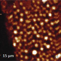
The KFM study showed that the surface topography is characterized by a number of pits of irregular shape that are scattered over the surface (Figure 12). The pit locations exhibit surface potentials which are 1V higher than the surrounding. The high surface potential patterns have a triangular shape.
The Raman scattering maps of the Si-C and Si bands are shown in Figures 12c-d and were collected on a larger area than the height and surface potential images. For comparison of the maps, the same AFM surface locations were marked by red squares.
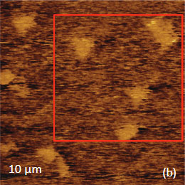
The fact that the contrast of Si-C band is much weaker than that of the Si band is consistent with the small thickness of Si-C film. The height image reflects the topography of the Si-C layer, whereas the optical micrograph and the Raman scattering maps refer to a bigger sampling volume that includes the underlying substrate defects. Due to the long-distant nature of electrostatic interactions, the surface potential contrast also provides sensitivity to the underlying substrate defects. This is another example how AFM and Raman studies complement each other.
CONCLUSIONS
Integrated AFM/Raman instrumentation will clearly bring important information to the understanding of materials especially on the micron scale and beyond. Chemical mapping based on Raman microscopy is an invaluable addition to AFM in combined AFM/Raman instruments. The presented data shows how this combination enhances comprehensive characterization of materials at small scales. Further progress in sensitivity and spatial resolution is expected with the advances in TERS tip technology. TERS has the potential to increase sensitivity and spatial resolution beyond the capabilities of conventional Raman microscopy. TERS studies will be covered in upcoming application notes.
REFERENCES
1. S. Magonov in Encyclopedia of Analytical Chemistry, (R. A. Meyers, Ed.), pp. 7432-7491, John Willey & Sons Ltd, Chichester (2000).
2. S. Magonov NT-MDT Application Note 084 (2012)
3. R. M. Stockle et al Chem. Phys. Lett. 318, 131 (2000)
4. S. Magonov NT-MDT Application Note 087 (2013)
5. M. Wall “Depth Profiling with Raman Microscope” Thermo Fisher Scientific Document.
6. U. Agarwal Planta 224, 1141-1153 (2006)
ACKNOWLEDGEMENTS
Our sincere thanks to Dr. U. Agarwal (USDA FS Forest Products Laboratory) for a sample of wood cells.