


High-Resolution Imaging in Different Atomic Force Microscopy Modes
Пример применений 088(pdf 1.7 Mb)
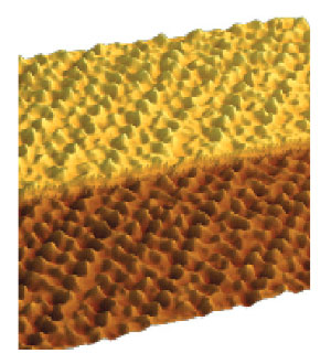
A bird-view on the terraces of calcite crystal
(6x11 nm) as imaged in water with Amplitude Modulation.
- An operation of AFM microscope in a temperature-stable cabinet facilitates high-resolution studies and makes molecular-scale imaging of different materials a routine procedure.
- The imaging at the atomic and molecular scale has been achieved on a number of samples not only in contact mode but also in the oscillatory resonant (Amplitude Modulation) and non-resonant (HybriD) modes.
- The tip-sample force interactions, which are different in the various AFM modes, help to visualize numerous types of adsorbate structures with the weakly-bonded adsorbates seen only in the oscillatory resonant mode.
John Alexander and Sergei Magonov
NT-MDT Development Inc. Tempe AZ USA
INTRODUCTION
High-resolution imaging is a primary function of Atomic Force Microscopy (AFM), and the related applications are continuously expanding with the ongoing instrumental developments. An operation at small scales (<100 nm) has a number of factors that influence the signal-to-noise ratio and spatial resolution of the images. The contrast of the height images reflecting sample topography is determined by the accuracy of the microscope feedback loop, which guides the response of the piezo scanner to the surface variations picked up by the tip-sample force interactions.
In contact and oscillatory modes, the feedback mechanism is based on different probe responses directly or indirectly related to the force interactions. The cantilever deflection is used for this purpose in contact and non-resonant oscillatory modes, and the amplitude or frequency changes of the interacting probe are employed for feedback in the oscillatory resonant modes. A bending of the probe to the set-point value is a relatively fast process, which proceeds in a quasi-static fashion in the contact mode. In the oscillatory non-resonant mode, such as HybriD (HD) mode, the probe deflects with 1-2 kHz rate, which is below the resonances of a vertical piezo-actuator and the probe. In both modes, the instant value of the deflection is measured and an error (a difference between the actual and set-point deflections) is eliminated by a Z-piezo motion that adjusts the probe-sample separation in the feedback operation.
This two-step process is characterized by a time constant, which is defined by the bandwidths of the detection and piezo-response. In contact mode, the piezo-scanner motion is actually the limiting factor because it is activated at the rate below the piezo-scanner resonance, which is around 10 kHz. Therefore, the vertical displacement with the rate of 5 kHz requires 200 microseconds to be executed at a single point. Therefore, 205 milliseconds are needed to perform this process in 1024 locations when this operation is performed in the single rastering line with 512 pixels per direction. In other words, the fastest scanning rate for 512 points-per-line imaging in the contact mode is around 5 Hz. At larger rates, the feedback will be executed poorly, and the profiling will be less precise. If the number of pixels is reduced then the spatial resolution will be hammered. In the HD mode, which typically operates at 1.5 kHz frequency, the deflection measurements are performed every ~0.7 milliseconds, and 0.68 second
is needed for the line with 512 pixels. This means that the fastest scanning rate for HybriD (HD) mode is ~1.5 Hz or slightly higher when the driving frequency is increased.
In the microscope operation in amplitude modulation (AM) mode, which is the resonant oscillatory method, the mechanical quality factor (Q) of the probe becomes an additional issue. When the probe has a resonance around 100 kHz and Q of several hundreds, the time to obtain an accurate amplitude value in a single point can be estimated as a time of 5 to 10 oscillations that is 10 to 20 kHz or 100 to 50 microseconds.
The Q-factor is also a source of delay as the probe moves from one position to another position on the surface, and it limits how fast the amplitude can adopt the change in surface interaction.
This will bring the maximum rate for scanning with 512 pixels per line to ~10 Hz. In practice, the rate needs to be reduced by approximately two times below the scanner resonance, which is around 10 kHz. This brings the maximum rate to ~5 Hz that is similar to the contact mode. Therefore, the above estimates showed that AFM measurements are relatively slow and the imaging rates should be further reduced when the surfaces have rough profiles.
The actual path of the probes while profiling the corrugated surfaces is much longer than one during scanning on atomically-smooth areas. When research demands a fast scanning operation then the special design of scanners, high frequency probes and various operation procedures are utilized for the practical realization of this function.
ELIMINATING THE THERMAL DRIFT OF AN AFM MICROSCOPE
One of the factors, which influences AFM imaging, is the thermal drift of the microscope. This becomes a hurdle when precise and high-resolution imaging is required, particularly, in studies at small scales. As we discussed above the scanning rates are quite limited, therefore, a special care should be taken to reduce the microscope thermal drift during the measurements. Temperature variations cause minor changes to the structural dimensions of microscope parts many of them being made of different
materials (aluminum, steel, titanium, ceramics, etc).
For example, a temperature variation of 1 °C causes a differential length change of the 1-cm Al and steel rods, as might occur using a steel lead screw in an aluminum stage (expansion of Al ~22 ppm/K, steel ~16 ppm/K) are around 60 nm. Therefore, to minimize the relative displacements of the microscope components while imaging samples with the atomic-scale resolution it is quite important to keep the temperature variations of the sample and the
probe well below the 0.01 °C level.
In the above example the temperature variations of 0.017 °C would give the 1-nm differential change. High temperature stability of the microscope has been achieved with the design of a special thermal cabinet, which in addition to the temperature stabilization incorporates other means for damping the acoustic and mechanical vibrations that are harmful to the AFM operation.
TEMPERATURE-STABLE CABINET
In the design of a microscope cabinet for low thermal drift operation we have considered the following issues. The AFM microscope has several internal sources of heat dissipation and the temperature at the sample location is usually 3-5 degrees higher than the room temperature (RT). Furthermore, when the microscope is placed in a closed environment it is heated as a whole. Having this in mind, we have decided to stabilize thermal environment of the microscope in the cabinet at elevated temperature level (2-3 degrees above RT).
The photograph in Figure 1 shows the external view of the cabinet. NT‑MDT SI microscopes: TITANIUM, NEXT and NTEGRA Prima can be placed inside the cabinet either on the vibration isolation structure held by 4 bungee cords attached to the cabinet ceiling or on the vibration isolation table installed on the cabinet floor. Several heating elements for controlling the temperature environment are placed inside the cabinet. The thermistors are mounted between two heat sinks, and vertical pipes, which are attached to the sinks, serve as the chimney above the heaters. These structures allow the air to flow off the bottom surface of the thermal cabinet through the heat sinks to the top of the cabinet. In this way gentle air circulation is enabled.
Temperatures of the room and the microscope frame near the sample location are monitored with the mounted semiconductor temperature sensors. The sensors’ readings are used for electronic feedback, which adjusts power to the heaters to keep the sample location temperature at the set-point value, which is a couple degrees above RT. This function is realized with a microprocessor, which also adjusts the set-point temperature when the RT changes substantially. The temperature readings are exhibited on the LCD display attached to the cabinet front.
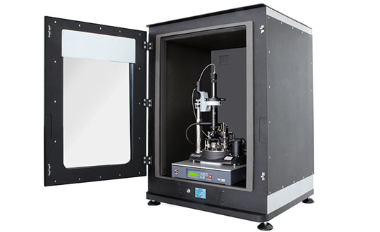
Figure 1. Thermal cabinet
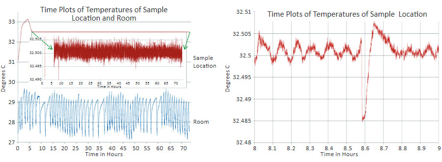
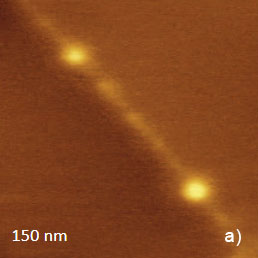
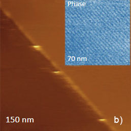
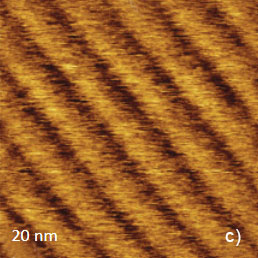
This chimney-like approach is very valuable because it does not require the use of fans, which are a non-desirable source of electric and mechanical disruptions during imaging. The temporal graphs in Figure 2a-b illustrate the temperature stability near the sample location as RT undergoes the 2-3 degrees variations reflecting the operation of the air-conditioner. After the microscope is placed into the cabinet and the heating is activated, the set-up period takes approximately 6 hours. Prior to stabilization at the set-point level, temperature of the microscope frame slightly overshoots it. Later on, the temperature variations around the set-point level are supported at the level of 0.005 °C. This is seen from the expanded view of the temperature changes, which is placed in the insert in Figure 2a. When the sample and the probe have been changed and the cabinet door is closed again, the temperature drop lasts only 10-15 minutes and afterwards the temperature returns to the set-point value, Figure 2b.
The temperature stability of our cabinet enables low-thermal drift AFM scanning, which is illustrated by a series of height images of the lamellar structure of semifluorinated alkanes in Figure 3. A small elevated defect, which is observed at the top left of the images, does not change its location in the consequent 100 nm scans. Thermal drift in these images is around 0.2 nm/min. This experimental data, which is described below, was obtained using the TITANIUM microscope equipped with electronic controllers enabling operation in contact mode and in oscillatory AM and HD modes. Our atomic-scale studies were made in air with Si probes: NSG01 (stiffness ~4 N/m) and NSG30 (stiffness ~40 N/m), with scanning rates up to 3 Hz and images of 512×512 pixels.
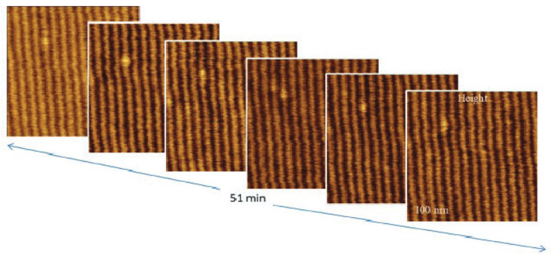
Figure 3. Height images of semi-fluorinated alkanes on graphite collected in sequential scans with 1 Hz scanning rate
ATOMIC-SCALE IMAGING IN CONTACT MODE
Since the early days of scanning probe microscopy high-resolution scanning tunneling microscopy (STM) and AFM imaging has been demonstrated on atomically-flat surfaces of layered materials, such as highly oriented pyrolitic graphite (HOPG), mica and dichalcogenides of transition metals MX2 (M = Mo, W, Ta, Ti, V; X = S, Se, Te). These materials can be easily cleaved and such freshly prepared surfaces are suitable objects for observation of the atomic-scale order. The examples of the AFM images of several layered materials in contact mode are collected in Figure 4. The height image of mica (Figure 4a) shows the periodical surface corrugations in the 0-0.1 nm range that precisely mimics the structure of the silicate mineral.
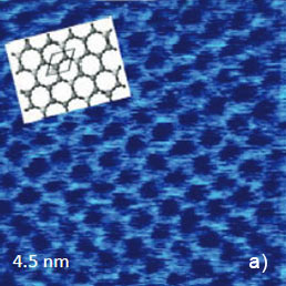
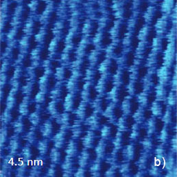
The overlay of a sketch of the surface structure on the image in Figure 4b confirms their close similarity. The periodic lattice of the image is characterized by a main period of 0.52 nm (the distance between the interatomic cavities), and this matches the crystallographic data. The atomic-scale images of mica are often used for a calibration of piezoelectric scanners. The pattern of the lateral force image is quite different with the elevations coinciding with the empty centers of the honeycombs in the height image. The AFM image, which was obtained in contact mode on the freshly cleaved surface of highly oriented pyrolitic graphite (HOPG), exhibits a hexagonal structure with much smaller spacing of 0.25 nm, Figure 5a.
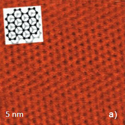
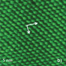
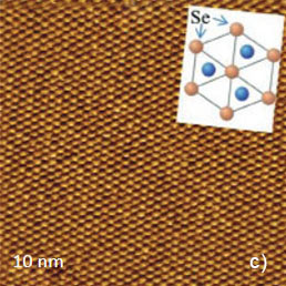
This arrangement is consistent with the pattern most commonly observed in STM images. Only three of six atoms forming a honeycomb cell are pronounced in the images [1]. This is explained by different strength of the neighboring C atoms in the honeycomb structure of this compound shown in the insert in Figure 5a. The contact mode images of two dichalcogenides of transition metals: WTe2 and MoSe2 (Figures 5b, c) match the crystallographic structures of the ab planes of these crystals. The rectangular pattern of height image of WTe2 [2] is consistent with the surface structure defined by the repeat distances of 0.63 nm and 0.35 nm in the orthogonal directions, the image in Figure 4b confirms their close similarity. The periodic lattice of the image is characterized by a main period of 0.52 nm (the distance between the interatomic cavities), and this matches the crystallographic data. The atomic-scale images of mica are often used for a calibration of piezoelectric scanners. The pattern of the lateral force image is quite different with the elevations coinciding with the empty centers of the honeycombs in the height image. The AFM image, which was obtained in contact mode on the freshly cleaved surface of highly oriented pyrolitic graphite (HOPG), exhibits a hexagonal structure with much smaller spacing of 0.25 nm, Figure 5a. This arrangement is consistent with the pattern most commonly observed in STM images. Only three of six which are indicated with the white arrows, Figure 5b. The hexagonal pattern of MoSe2 image is consistent with the central hexagonal symmetry of this crystal, Figure 5c. The main spacing of 0.32 nm is also close to the crystallographic data.
The above images of layered materials were obtained in contact mode at ambient conditions with the probes having stiffness as high as 40 N/m. The attempt to get similar images in AM and HD modes was not successful, most likely, due to weakly bonded surface contaminations, which were found even on freshly cleaved surfaces of these materials. Presumably, in contact mode the contaminations are brushed away, but this does not occur in the modes with relatively low level of lateral forces. Further work to overcome this hurdle is in progress.
The above images of layered materials were obtained in contact mode at ambient conditions with the probes having stiffness as high as 40 N/m. The attempt to get similar images in AM and HD modes was not successful, most likely, due to weakly bonded surface contaminations, which were found even on freshly cleaved surfaces of these materials. Presumably, in contact mode the contaminations are brushed away, but this does not occur in the modes with relatively low level of lateral forces. Further work to overcome this hurdle is in progress.
VISUALIZATION OF THE MOLECULAR STRUCTURE OF ORGANIC CRYSTALS
A number of organic crystals also have a layered structure and their fresh crystalline surfaces can be obtained by a cleavage with sticky tape. One of such crystals is a charge transfer compound of TTF-TCNQ (where TTF – tetrathiafulvalene and TCNQ – tetracyanoquinodimethane), the first synthesized molecular conductor. This crystal is built of alternative stacks of partially negative TTF molecules and partially positive TCNQ molecules, with the latter serving as conducting paths formed of the edge-on standing molecules with overlapping conjugated moieties.
The crystallographic structure of the largest face being the bc plane of TTF-TCNQ salt is shown in Figure 6a. The repeat distance along the stacks is 0.38 nm (the crystallographic b-constant) and the repeat distance in the orthogonal direction is the combined width of the anion and cation stacks of 1.2 nm (the crystallographic c-constant). The visualization of the molecular arrangement at this surface was first achieved in STM [3]. The atomic-scale STM images exhibit a complex periodical pattern, which is consistent with the ab unit cell. The individual features within the unit cell reflect a partial electron density map at the conducting molecular orbital level, which is dominated by contribution of TCNQ molecular orbitals [4]. The earlier AFM images of the same surface obtained in the contact mode showed the periodical pattern, which is also consistent with the periodical spacings of the ab plane.
The fine periodical structure, when recovered by fast Fourier Transform (FFT) filtering of the image, has been different from the one recorded in the STM image. The rational explanation of the AFM pattern was achieved from its match with the map of total electron density of the molecular structure at this plane [4]. The contact mode AFM images of TTF-TCNQ crystal, which were recorded in the thermally-stable cabinet with the 2 Hz rate, are shown in Figure 6b-c.
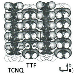
These images are characterized by a relatively high signal-to-noise ratio and visualization of the atomic-scale features does not require FFT filtering. The image details are consistent with the molecular structure of the ab plane as shown by the overlayer in Figure 6c. The top close positioned atoms of TTF stacks most likely correspond to the elevated rows in the images. A pair of cyano end groups of TCNQ molecules in the stacks matches to the slightly depressed rows in between the elevated rows assigned to the TTF stacks. The visualization of the molecular order at the bc plane of this crystal has been also achieved in the image, which was obtained in AM mode (Figure 6d), yet the fine details are not well distinguished.
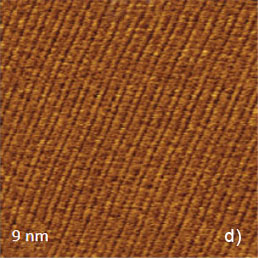
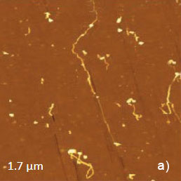
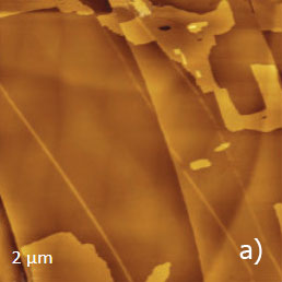
Polydiacetylene (PDA) polymers are prepared by the solid-state polymerization induced by heat or light. We have examined one of polymers – 2,4-hexadiynylene bis(p-fluorobenzenesulfonate). The crystallographic structure of the monomer crystal brings close the triple bonds of different molecules, which are arranged in a layered fashion parallel to the largest surface of the lozengeshaped crystals (the bc crystallographic plane). The polymer chains are formed inside the monomer crystal and the conversion of triple bonds to double bonds in polymer involves only small structural rearrangements. Therefore, the structures of such polymer and monomer crystals are quite similar and the lozenge shape does not deteriorate by polymerization. Yet the difference of the crystals is revealed by a cleavage, which in the case of the polymer produces some fibrils split from the crystal, Figure 7a.
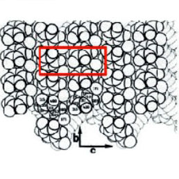
The fibrils are oriented along the short diagonal of the lozenge, and they should be avoided by the scanning probe during imaging. The crystallographic structure of the bc face of PDA is presented in Figure 7b. The surface molecular arrangement is characterized by the stacks of the polymer side groups, which are aligned along the b direction. In the adjacent rows of phenyl rings along this axis, the rings are oppositely oriented. Therefore, the unit cell with the constants b = 0.53 nm and c = 1.62 nm includes molecules of two rows.
The contact mode image of PDA crystal, which was obtained on the bc plane, shows a periodical pattern (Figure 7c) with a higher quality than that published previously [5]. Again, FFT filtering was not needed for the visualization of the atomicscale details. There is a good correspondence between this image and the molecular crystallographic structure of this plane under the assumption that top adjacent hydrogen atoms of the phenyl rings of each molecule correspond to a single bright spot in the image.
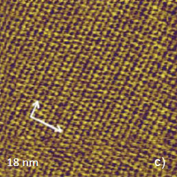
Several molecular-scale images of PDA crystal were recorded in the AM mode, Figures 8a-b. The larger-scale patterns show the main periodical features with several defects, which might originate during the cleavage. The image resolution in Figure 8a is slightly worse than the one obtained in the contact mode. Nevertheless, the higher magnification image in Figure 8b shows the individual patterns that can be assigned to the phenyl rings of the molecular stacks.
SURFACE ORDER OF ALKANES AND ALKANOLS ON DIFFERENT SUBSTRATES
The examination of molecular ordering in adsorbates on different substrates is one of the research areas of STM and AFM. The molecular- and atomic-resolution STM images of the organic compounds, which include normal alkanes and their derivatives, were obtained using droplets of saturated solutions of the compounds deposited on HOPG.
In these experiments the conducting probe penetrates through a weakly-bonded and nonconducting adsorbate until it collects tunneling current variations Surface Order of Alkanes and Alkanols on Different Substrates at the molecular layer immediately lying on a conducting substrate [6]. In case of normal alkanes, the STM image reveals not only the lamellar order of flat-lying molecules but also its conformational order, in which the -CH2-CH2-CH2- zigzag either lies flat or stays
perpendicular to the substrate.
The situation is different when the imaging is performed on dry adsorbate that can be examined only with AFM. We have performed studies of samples of several normal alkanes C18H38, C22H46, C36H74 and dodecanol C12H26O on HOPG and MoS2 using different AFM modes.
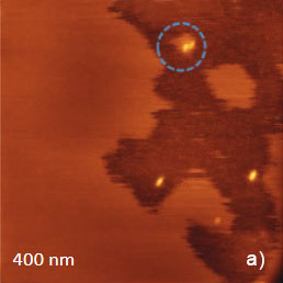
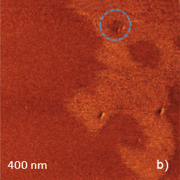
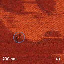
AFM images of dodecanol adsorbate on MoS2 were first collected in the AM mode, Figure 9a‑c. The left part of the height image (~400-nm surface area) is covered by a feature-less layer, which is ~0.5 nm in height, Figure 9a. Therefore, this overlayer and its few separate patches can be assigned to the top molecular layer without a noticeable in-plane order. The darker areas on the right represent the bottom layer, in which traces of lamellae with spacing of ~3.3 nm are distinguished in the phase image
(Figure 9b). The top layer is weakly bonded and the shape of its domains is influenced by the tip force during scanning. As a result of a competition between the tip-sample force interactions and the self-assembly of dodecanol molecules this layer seems to be “mobile”. This is evidenced by a change of the surface morphology near the particles marked with a blue circle in Figure 9a‑c.
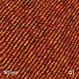
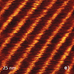
The 200-nm phase image in Figure 9c more clearly shows the region with the lamellar structures of the bottom layer. When the similar area is examined with HD mode using the same probe as in the AM mode study, the top layer was not noticed and the images show only lamellar structures of dodecanol, Figure 9d‑e. The tip-force applied in HD mode was 1 nN.
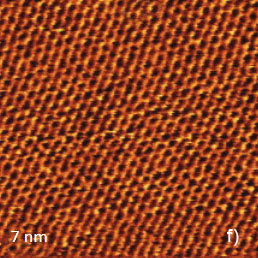
Furthermore, the imaging of the dodecanol adsorbate with contact mode using the same probe revealed the molecular structure of MoS2 with the hexagonal symmetry and main spacing of 0.32 nm, Figure 9f. In other words, the probe operating in contact mode brushed away the organic adsorbate and the tip interacts with the substrate. This example demonstrates that a combined use of different AFM modes, which are characterized by different level of the probesample forces, brings the complimentary information
about the sample organization.
The observation of the lamellar order of C12H26O, which bulk melting point is around 25 °C, at 30 °C can be explained by the epitaxially-induced order on MoS2. The same is true for the AFM observations of the lamellar order of normal alkanes (from C16H34 to C392H782) on HOPG [8, 9]. The related samples of alkanes started from C18H38 can be prepared by a heating of a small crystal of the alkanes on HOPG to temperature 20-30 degrees above its melting point and back to room temperature.
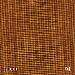
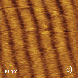
At high temperature the alkane melt flows over the surface and on cooling the material assembles into large crystalline aggregates leaving some material on the surface nearby them. These areas are usually covered by the lamellar layers and the lamellae at the melt/HOPG interface retain their order at temperatures 20-30 degrees above the melting temperatures of their crystals [10]. Specifics of the AFM observations of alkane layers on HOPG are demonstrated in our study of C22H46 and C36H74 adsorbates. Height image of the C22H46 adsorbate, which covers an HOPG step, was collected in AM mode, Figure 10a.
Several alkane droplets are condensed at the terrace’s edge. This image has been obtained in low-force imaging as documented by a featureless phase image (not shown here). With the increase of the tip-force, which is achieved by the lowering of the amplitude set-point, the droplets were removed, and the traces of lamellar structures became evident on lower and higher terraces, Figure 10b. The lamellar structure is best resolved in the phase image, which is shown as an overlay on the height image in Figure 10b. The lamellar structure has been well resolved in the images obtained with the same probe in HD mode.
The related height image showing several individual C22H46
lamellae with the spacing of 3.1 nm is presented in Figure 10c. The adsorbate of longer alkane: C36H74 (with melting temperature of 75 °C) exhibits surface layered structures, which are 0.5 nm in height. Therefore, they can be assigned to the lamellar sheets with molecules lying parallel to the substrate, Figure 11a.
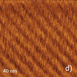
At smaller scans the lamellar structures are well distinguished in the images obtained in AM and HD modes. In both modes, the imaging might be destructive and a partial removal of the alkane molecules from the lamellar sheets has been observed. The related dark vacancies, which are extended perpendicular to the lamellae edges, are observed in the height images recorded in HD mode, Figures 11b-c. The number of the damaged locations has risen with the downsizing of the imaging area due to the effective increase
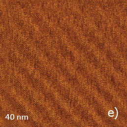
tip-sample force interactions. The alkane layers lying closer to the substrate are more resistive to the tip-induced damage and, they can be examined in contact mode, Figure 11d‑e.
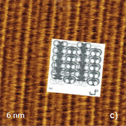
A couple of decades ago, the alkane lamellae at the interface between a saturated alkane solution and HOPG were examined with scanning tunneling microscopy (STM). STM images provided the high-resolution visualization of individual alkane chains, which form the lamellae by packing in the normal direction to the lamellar edges. A comparable resolution has not yet been achieved in routine AFM imaging. The hints of the chain ordering were noticed in the images of C36H74 lamellae, which were
recorded in contact mode, Figure 11d‑e.
Multiple fine striations, which are aligned perpendicular to the lamellar structures, are distinguished in both images. Their order has a periodical spacing of 0.5 nm, which correlates well with the inter-chain packing in the alkane crystals, and is better resolved in the lateral force image. These images provide support of the earlier finding of chain resolution in the contact mode study of a similar sample [11].
MORPHOLOGY AND CHAIN ORDER IN ORIENTED POLYTETRAFLUOROETHYLENE
Poly(tetrafluoroethylene) – PTFE is a widely known fluorinated polymer with a large variety of technological applications. Rubbing of PTFE on a rigid substrate (glass, Si, etc.) at high temperature leads to deposition of the polymer and its orientation. This surface is often used for aligning liquid crystalline materials and for epitaxial crystallization of low and high molecular weight compounds. For AFM studies we prepared such oriented PTFE layer on a glass substrate and performed its imaging in different modes.
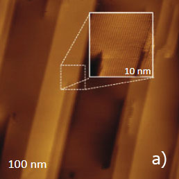
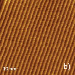
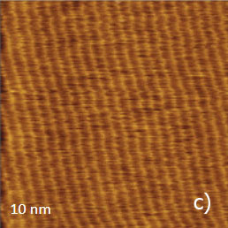
The height image of this sample, which was recorded in AM mode, is shown in Figure 12a. The surface is formed of multiple ribbons, which are aligned along the rubbing direction. The smallest steps between the neighboring ribbons are around 0.5 nm that hints that they consist of molecular sheets of PTFE. The 10-nm image of the surface location nearby one of the surface defects is shown in the insert in Figure 12a.
This image exhibits the well-oriented linear elevated features with a separation of 0.6 nm, which is close to the inter-chain distance of 0.56 nm in oriented and crystalline PTFE samples examined by other methods (TEM, X-ray analysis). Therefore, the observed pattern represents the molecular alignment of the polymer chains. A similar pattern has been recorded in other flat locations of the sample in the 10-nm images obtained in AM and contact modes, Figure 12b-c. In fact, the capability of the visualization of the PTFE chains in the contact mode was demonstrated a long time ago [12], whereas the molecular resolution images in AM mode are relatively new. The same PTFE sample has been also examined with HD mode, Figure 13a-e.
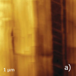
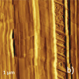
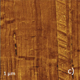
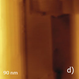
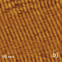
The vertically oriented strands, which are visualized in the 1-micron images, are split into extended blocks of several hundreds of nanometers in length. These structures, which are better distinguished in the phase image, are similar to the crystalline domains with extended polymer chains. The highpressure crystallized polyethylene and samples of polyolefins epitaxially crystallized on atomically-smooth substrates exhibit similar morphology. The smaller 90-nm image shows an extended crystalline
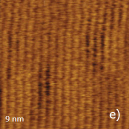
block surrounded by protrusions with multiple steps, Figure 13d.
The imaging of the flat surface of this block revealed the aligned polymer chains with the inter-chain
distance of 0.56 nm, Figure 13e. The examination of the rubbed PTFE sample has demonstrated the molecular chain visualization in all three AFM modes.
An open question is the capability to visualize the conformation of these macromolecular chains, which adopt 13/7 and 15/7 helices at temperatures below 19 °C and 28 °C, respectively. Unfortunately, the above described measurements were performed at higher temperature (~30 °C) and the visualization of PTFE conformations is one of the next challenges to address.
COMMENTS ON ATOMIC-SCALE AFM IMAGING
Despite the progress in AFM imaging with atomic-scale resolution, its nature is not well understood. When the images reproducing the lattices of crystalline samples were recorded in contact mode, the researchers did not find any point defects (e.g. vacancies in the lattices), in contrast to STM images that are full of atomic-scale imperfections.
Therefore, a visualization of the single-atom defects has been considered as evidence of true atomic resolution. The AFM images showing such defects were first obtained in the resonance frequency modulation mode in vacuum and later in AM in air [13]. Generally, the improvement of the signal to noise ratio in AFM microscopes, which allows the low-amplitude (less than 1 nm) operation in AM and FM modes helps to achieve the atomic-scale resolution on crystalline surfaces and on DNA strands in water.
One of the related issues - a reduction of tip-sample forces makes the contact area smaller than the tip apex. This might explain that the atomic-resolution images were recorded with the tips having a radius around 10 nm. As regarding imaging in air, the samples can be covered by a contamination overlayer, and an operation at larger amplitudes might be needed for the tip apex to touch a surface of interest. Therefore, the images illustrated in this note were obtained with the amplitudes in the 5-20 nm range using common Si probes (NT‑MDT SI probes: NSG01, NSG10 and NSG30) with the tip radius around 10 nm. The visualization of the atomic-scale features assumes that the effective contact area is rather small.
Some clues regarding the atomic-scale visualization were provided by theoretical calculations of the images for a model compound the crystal structure of PDA with missing molecule [14]. It has been shown that the defective structure is correctly reproduced only when the atomically-sharp tip interacts with the sample at the minimal forces. As the tip-force and tip-radius increase the image pattern changes yet the defect is still present. The surface corrugations become smaller and beyond the detection limit (~0.01 nm) as the tip radius increases above 20 nm.
In general, the high-resolution imaging is the microscope function that depends on several instrumental and operation factors. They include not only the described measurements in thermally stable environment but also the precise force control, especially, in the low-force region, and dimensions of the tip apex. Furthermore, the imaging media and nature of the sample are also very essential for the success of the experiments at the atomic- and molecular-scale. A full control of these factors is the only way for a better understanding the capabilities of AFM high-resolution studies.
CONCLUSIONS
The operation of AFM in low temperature drift environment facilitates high resolution studies at small scales. Visualization of atomic and molecular structures becomes a routine procedure in contact, AM and HD modes. This is confirmed in the studies of inorganic layered materials, organic crystals, polymers and adsorbates. The atomic and molecular scale images of these materials were recorded using regular Si probes. The different level of tip-sample forces in the different AFM modes allows expanding the technique access to a broader range of surface structures as demonstrated in the study of dodecanol adsorbates on MoS2. In a further step the small-scale visualization studies will be expanded to probing of the local mechanical and electric properties with high spatial resolution.
REFERENCES
[1] J. M. Soler, A. M. Baro, N. Garcia, and H. Rohrer “Interatomic Forces in Scanning Tunneling Microscopy: Giant Corrugations of the Graphite Surface” Phys. Rev. Lett. 57, 444-447 (1986)
[2] S. W. Hla, V. Marinkovic, A. Prodan, and I. Musevic “STM/AFM investigations of β-MoTe2, α-MoTe2 and WTe2” Surf. Sci. 352-354, 105-111 (1996)
[3] T. Sleator and R. Tycko “Observation of individual organic molecules at a crystal surface with use of a scanning tunneling microscope” Phys. Rev. Lett. 60, 1418-1421 (1988)
[4] S. N. Magonov, G. Bar, H.-J. Cantow, J. Ren, and M.-H. Whangbo “Interpretation of scanning tunneling and atomic force microscopy images of TCNQ salts” Synthetic Metals 62, 159-167 (1994)
[5] S. N. Magonov, G. Bar, H.-J. Cantow, H.-D. Bauer, I. Mueller, and M. Schwoerer “Atomic force microscopy of polymers and polymer related compounds 3. Monocrystals of monomer and polymer 2,4-hexadiynylene bis(p-fluorobenzenesulfonate) Polym. Bull. 29, 223-230 (1991)
[6] G. C. McGonigal, R. H. Bernhard and D. J. Thomson “Imaging alkane layers at the liquid/graphite interface with the scanning tunneling microscope” Appl. Phys. Lett. 57, 2828-2830 (1990)
[7] C. L. Claypool, F. Faglioni, W. A. Goddard III, H. B. Gray, N. S. Lewis, and R. A. Marcus “Source of Image Contrast in STM Images of Functionalized Alkanes on Graphite: A Systematic Functional Group Approach” J. Phys. Chem. B 101, 5978-5995 (1997)
[8] L. Pham Van, V. Kyrylyuk, J. Polesel-Maris, F. Thoyer, C. Lubin, and J. Cousty “Experimental Three-Dimensional Description of the Liquid Hexadecane/Graphite Interface” Langmuir 25, 639-642 (2009)
[9] S. N. Magonov, N. A. Yerina, G. Ungar, D. H. Reneker, and D. A. Ivanov “Visualization of Lamellae Thickening during Thermal Annealing of Single Crystals of Ultra Long Alkane (C390H782) and Polyethylene” Macromolecules 36, 5637-5649 (2003)
[10] S. N. Magonov, and N. A. Yerina “High Temperature Atomic Force Microscopy of Normal Alkane C60H122 Films on Graphite” Langmuir 19, 500-504
(2003)
[11] G. Valdre, A. Allessandrini, U. Muscatello, and U. Valdre “High-Resolution Imaging of N-Alkane Crystals by Atomic Force Microscopy” Phil. Mag. Lett. 78, 255-261 (1998)
[12] S. N. Magonov, S. Kempf, M. Kimmig, and H.-J. Cantow “AFM on Polymers and Polymer Related Compounds 4. Polytetrafluoroethylene and Polycarbonate” Polym. Bull. 26, 715-722 (1991)
[13] D. Klinov, and S. Magonov “True Molecular Resolution in Tapping Mode Atomic Force Microscopy” Appl. Phys. Lett. 84, 2697-2699 (2004)
[14] S. Belikov, and S. Magonov “True Molecular-Scale Imaging in Atomic Force Microscopy: Experiment and Modeling” Jap. Jour. Appl. Phys. 45, 2158-2165 (2006)